Introduction of IODIR,PINSEL,IOSET and IOCLR Registers
How to select the direction of the port?
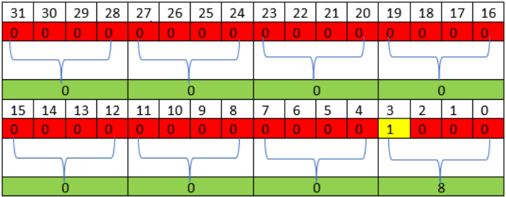
IODIR is the command used to set the direction of the port as an input or an output. For setting the pin as an input pin we need to provide logic 0 and for setting the pin as an output pin we need to provide logic 1 to the respective pin. By default, on reset, all the pins are acting as an input so there is no need to set the pin as an input pin if we are resetting the arm7. But for setting the pin as an output pin we need to provide logic 0. Let's take the below example:
Supposed I want to set pin 3 of port 0 as an output then I will provide logic 1 to pin 3 of port 0.
IODIR0:

IODIR0 = 0x00000008
Supposed I want to set pin 16, pin 15, pin 2 and pin 1 of port 1 as an output then I will change the bits as follows:
IODIR0 = 0x00018006;
How to select the pin for a particular function?
In arm7 each pin has multiple functions, to select the particular function of the respective pin PINSEL register is used. To select the particular function in the pin we need to provide 00,01,10,11 in a sequence to that particular pin.
In ARM 7 there are three PINSEL register dedicated to the
particular set of the pins as follows:
PINSEL0: P0.15 to P0.0
PINSEL1: P0.31 to P0.16
PINSEL2: P1.16 to P1.31
To understand it more clearly, let’s take an example of pin
27 which is having 4 functions as mentioned below:
P0.4: General purpose digital input/output pin
SCK0: Serial clock for SPI0.SPI clock output from a master
CAP0.1: Capture input for Timer 0, channel 0
AD0.6: A/D converter 0, input 6
To select among the four functions, we have to provide the
following data to the respective pin as mentioned below:
|
P0.4 |
SCK0 |
CAP0.1 |
AD0.6 |
|
00 |
01 |
10 |
11 |
Supposed I want to used pin 27 as an ADC pin, then as this pin is P0.4 pin I will use PINSEL0.
To select
the ADC function of this pin we need to provide following data to PINSEL0
register.
PINSEL0 =
0x00000300;(To select the pin function as adc pin we need to provide this data
to PINSEL0 register)
To
understand it more clearly, let’s take the example of pin 13, pin 9, and pin
52.
Pin 13: P0.28/AD0.1/CAP0.2/MAT0.2
Pin 9: P0.25/AD0.4/AOUT
Pin 52: P1.30/TMS
Supposed I
want to use pin 13 as a general-purpose input/output pin, pin 9 as an aout pin
i.e. D/A converter output, and pin 52 as a TMS(Test mode select for JTAG
interface) pin.
To select
the required function for the above pins I will provide 00,01,10,11
sequentially to the respective pin and select the required function of that
pin.
PIN 13:
|
P0.28 |
AD0.1 |
CAP0.2 |
MAT0.2 |
|
00 |
01 |
10 |
11 |
Configuration of PINSEL1 register for pin 13 to be used as an general purpose input/output pin as follows:
PINSEL1
= 0x00000000;
PIN 9:
|
P0.25 |
AD0.4 |
ADOUT |
|
00 |
01 |
10 |
Configuration of PINSEL2 register for pin 9 to be used as an AOUT(DAC output) pin as follows:
PINSEL1 = 0x00200000;|
P1.30 |
TMS |
|
00 |
01 |
Configuration
of PINSEL2 register for pin 52 to be used as an TMS(Test mode select for JTAG
interface) pin is as follows:
IOSET and IOCLR Registers :
IOSETx:
Here x represents the port number. This register is used to set the particular pin of the respective port. Providing logic 1 will set the pin and providing logic 0 does not affect the pin.
For example, If I want to set the port1.31 pin then I will provide the following data to the IOSET1 register:
IOSET1=0x10000000;
IOCLRx:
Here x represents the port number. This register is used to clear the particular pin of the respective port. Providing logic 1 will clear the pin and providing logic 0 does not affect the pin.
For example, If I want to clear the port1.31 pin then I will provide the following data to the IOCLR1 register:
IOCLR1=0x10000000;


Comments
Post a Comment